
Introduction to Multilayer Silicon Photonics
Silicon photonics, a technology that combines silicon-based electronic circuits with photonic devices, is rapidly transforming the landscape of data communications, sensing, and integrated optics. The multilayer silicon photonics platform represents a significant leap forward by enabling the integration of various optical components onto a single chip, enhancing functionality while maintaining compatibility with established CMOS fabrication processes.
The Evolution of Silicon Photonics
The journey of silicon photonics began in the early 2000s when researchers realized the potential of silicon as a medium for optical waveguides. Initial developments focused on creating basic photonic devices, such as waveguides and modulators. However, as the demand for high-speed data transmission grew, so did the need for more complex integrated circuits capable of handling increased data loads.
Early Developments
In the early phases, silicon photonics struggled with scalability and integration challenges. The lack of a suitable fabrication process that could accommodate the intricate designs of photonic devices alongside traditional electronic components was a significant barrier. However, the advent of multilayer structures has opened new avenues for overcoming these hurdles.
Advancements in Multilayer Structures
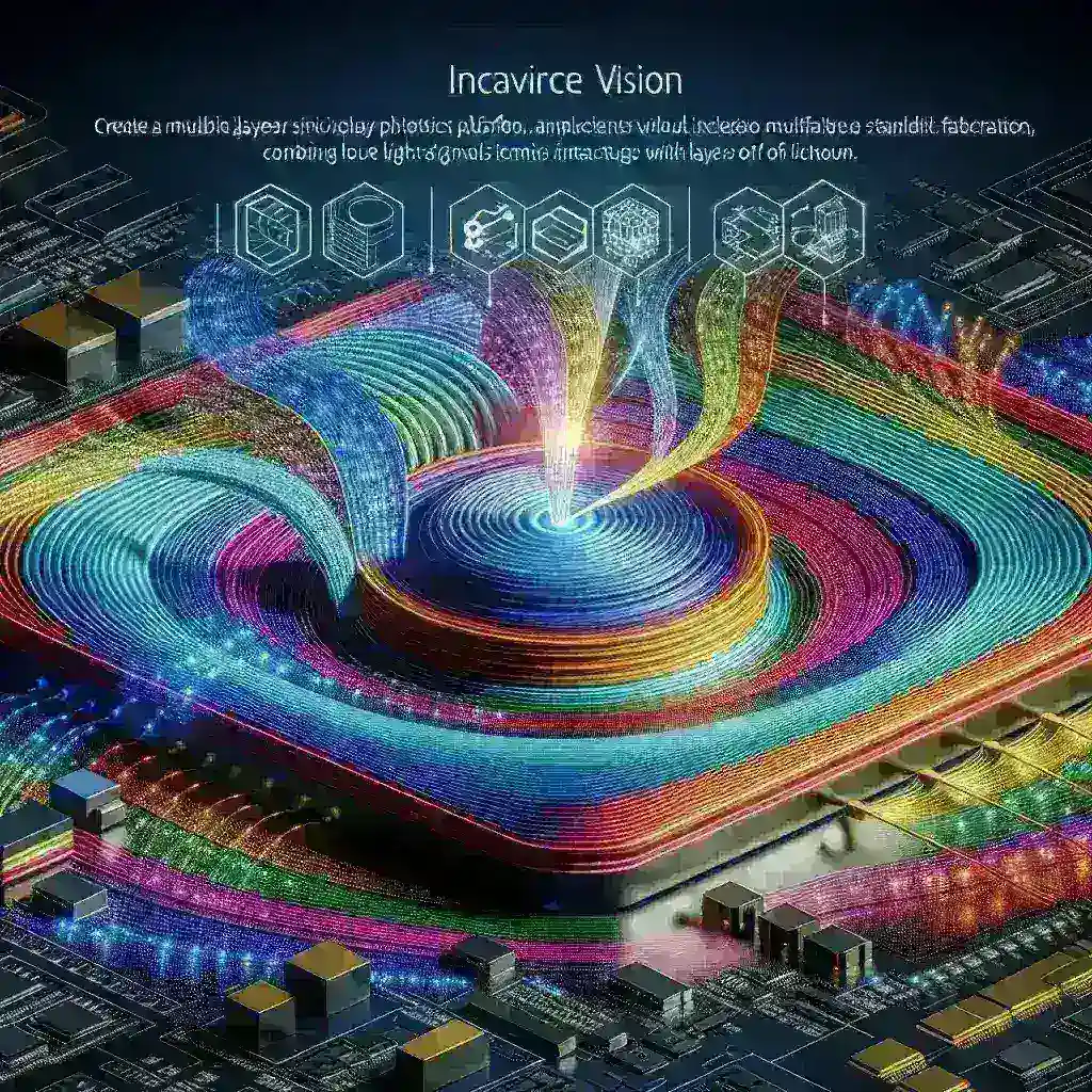
Multilayer silicon photonics technology involves stacking multiple layers of silicon and other materials to create a more versatile platform for photonic devices. This approach allows for the integration of various functionalities, such as optical waveguides, modulators, detectors, and lasers, all on a single chip.
Integration with Standard CMOS Fabrication
One of the most significant advantages of multilayer silicon photonics is its compatibility with standard CMOS fabrication techniques. CMOS (Complementary Metal-Oxide-Semiconductor) technology is the backbone of modern electronics, widely used in the production of microchips. The integration of multilayer silicon photonics with standard CMOS processes allows manufacturers to leverage existing infrastructure, reducing production costs and time-to-market.
Benefits of Integration
- Cost Efficiency: By utilizing established CMOS fabrication techniques, companies can significantly reduce the costs associated with developing new manufacturing processes for photonic devices.
- Scalability: The ability to produce large quantities of photonic integrated circuits using standard methods facilitates scalability, which is crucial for meeting the demands of the technology market.
- Enhanced Performance: The combination of optical and electronic functionalities on a single chip enhances overall performance, enabling faster data transmission rates and reduced power consumption.
Applications of Multilayer Silicon Photonics
Multilayer silicon photonics platforms have a wide array of applications, significantly impacting various industries, including telecommunications, medical technology, and consumer electronics.
Telecommunications
The demand for higher data rates and bandwidth in telecommunications networks has led to the adoption of silicon photonics for high-speed optical interconnects. Multilayer platforms can integrate multiple optical functions necessary for routing and processing data, facilitating efficient communication over long distances.
Medical Technology
In the medical field, silicon photonics can be utilized for advanced imaging and sensing applications. Photonic devices integrated into medical instruments can provide real-time data with high precision, improving diagnostics and treatment outcomes.
Consumer Electronics
Consumer electronics are also benefiting from advancements in silicon photonics. Products such as smart devices and wearables are increasingly incorporating photonic technologies to enhance functionalities, improve battery life, and deliver superior performance.
Challenges and Considerations
Despite its many advantages, the integration of multilayer silicon photonics with standard CMOS fabrication does present certain challenges that must be addressed.
Material Compatibility
Ensuring compatibility between the various layers of materials used in multilayer structures can be complex. Research is ongoing to identify suitable materials that can be integrated without compromising performance.
Thermal Management
As the density of components increases on a silicon photonics chip, managing heat becomes crucial. Effective thermal management solutions must be developed to prevent overheating and ensure reliable operation.
Design Complexity
The design process for multilayer silicon photonics can be significantly more complex than traditional silicon designs. Advanced simulation and modeling tools are needed to optimize device performance and integration.
The Future of Multilayer Silicon Photonics
The future of multilayer silicon photonics platforms looks promising, with ongoing research and development paving the way for further advancements. As the technology matures, we can expect to see even greater integration of optical and electronic components, leading to more sophisticated applications across various industries.
Predictions for the Next Decade
Experts predict that within the next decade, multilayer silicon photonics will become the standard for many applications, particularly in high-speed data communications and advanced sensor technologies. The continuous push for miniaturization and increased functionality will drive innovation in this field.
Conclusion
The integration of multilayer silicon photonics with standard CMOS fabrication marks a significant milestone in the evolution of photonic technology. By leveraging existing manufacturing processes and enhancing functionality, this innovative platform is set to revolutionize various industries. As researchers and manufacturers continue to explore the potential of this technology, we can expect to see a profound transformation in how we transmit, process, and utilize data.
In summary, the multilayer silicon photonics platform not only enhances the capabilities of photonic devices but also aligns with the existing CMOS infrastructure, making it a key player in the future of high-tech applications.